A1.1.4 Explain the purposes of different types of primary memory.
• Random-access memory (RAM), read only memory (ROM), cache (L1, L2, L3), registers
• The interaction of the CPU with different types of memory to optimize performance
• The relevance of the terms “cache miss” and “cache hit”
📚 You can find additional information in the course companion pages 12 to 15
The Big Idea
Primary memory, also known as main memory, is an important component in any computing system. It directly supports the execution of programs by providing the CPU with fast and flexible access to instructions and data. However, not all primary memory is equal—different types serve distinct purposes, trade-offs, and performance characteristics.
This article explores the four key types of primary memory—RAM, ROM, cache (L1, L2, L3), and registers—and explains how the CPU interacts with them to optimize performance. We'll also clarify important concepts such as cache hits and cache misses, which are central to understanding how modern processors manage memory access efficiently.
There is an article here which dives into depth about primary memory.
And this is an article which details L1, L2, and L3 cache's in great detail. You should read both articles.
Random-Access Memory (RAM)
RAM is volatile memory used as the main working area of the computer during execution. Programs, the operating system, and active data are loaded into RAM so that the CPU can access them quickly.
- Volatile: Loses contents when power is turned off.
- Read/Write: The CPU can read from and write to RAM.
- Speed: Slower than cache and registers, but faster than secondary storage (e.g., SSD).
RAM is organized in a flat memory model and is managed by the operating system's memory management unit. Accessing RAM generally takes tens to hundreds of nanoseconds, making it relatively slow from the CPU’s perspective.
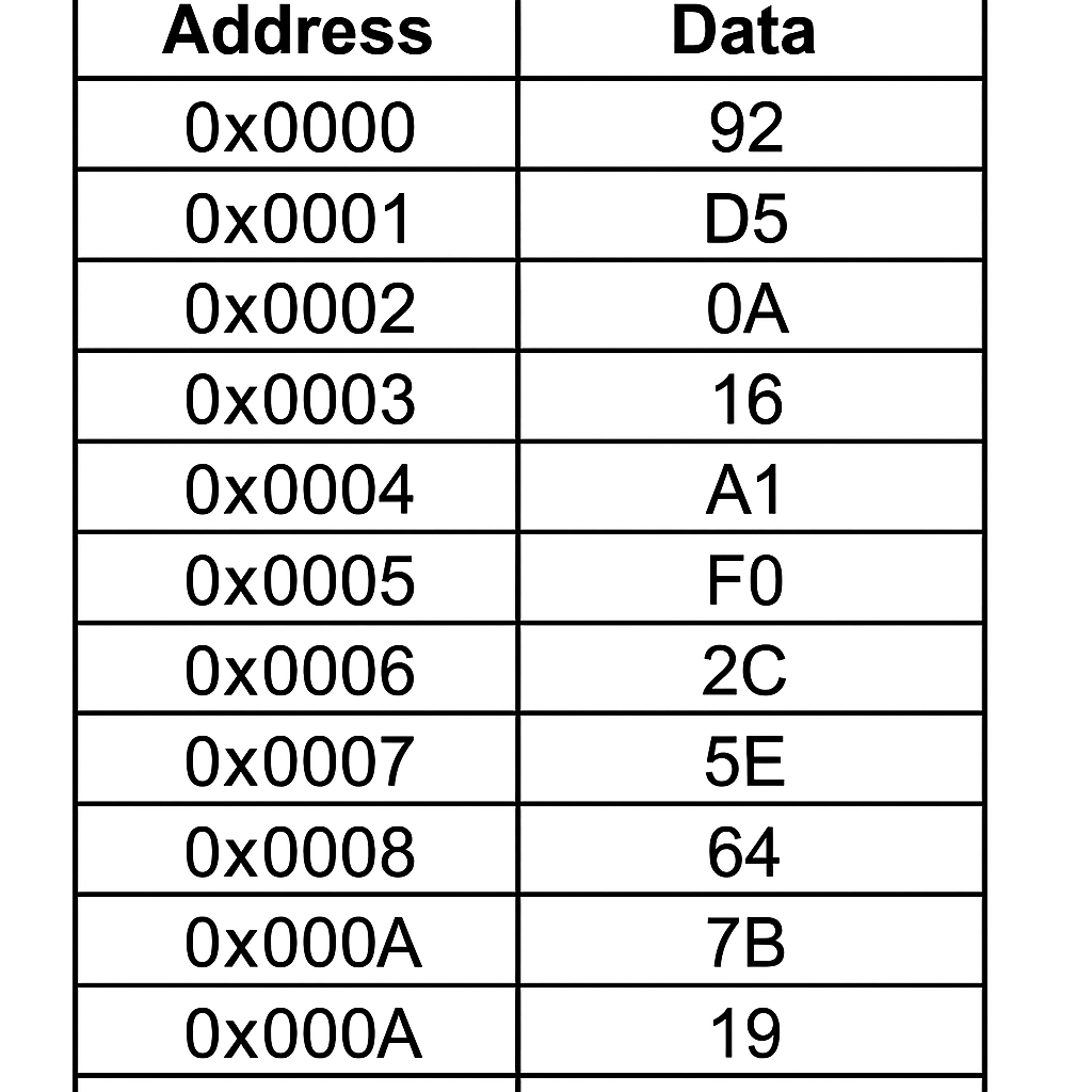
Please remember in primary memory, the address is not one byte. The data stored at that address is one byte.
- An address is just a number used by the CPU to locate data in memory.
- On a 32-bit system, an address is 32 bits.
- On a 64-bit system, an address is 64 bits.
- The width of the address has nothing to do with how many bytes it stores.
- The memory cell located at each address contains exactly one byte of data.
This is what “byte-addressable memory” means: every unique address identifies one byte of storage.
Read-Only Memory (ROM)
ROM is non-volatile memory that stores fixed, read-only data, often used for firmware.
- Non-volatile: Retains data when power is off.
- Read-only: Data is written at manufacture or through special programming techniques.
- Usage: Stores BIOS/UEFI firmware, system initialization routines, and low-level hardware configuration.
ROM is typically accessed only during boot processes or hardware diagnostics, not during general-purpose program execution. A student asked where changes are saved when you alter ROM (for example, the boot order). The answer to this excellent question is linked here.
Cache Memory (L1, L2, L3)
Cache is a small, high-speed memory located close to the CPU cores. It stores copies of data from frequently used RAM locations to reduce latency.
Cache levels:
| Level | Size | Speed | Location |
|---|---|---|---|
| L1 Cache | Smallest (e.g., 32 KB) | Fastest (~1–2 cycles) | Inside each CPU core |
| L2 Cache | Larger (e.g., 256 KB) | Slightly slower (~3–14 cycles) | Per core or shared |
| L3 Cache | Largest (e.g., 8–32 MB) | Slowest (~30–50+ cycles) | Shared between all cores |
Caches are managed by the cache controller, which uses algorithms like Least Recently Used (LRU) to determine which data to keep or evict. Caches are organized in lines (usually 64 bytes) and may be write-back or write-through, depending on how they synchronize with main memory.
CPU Registers
Registers are the fastest and smallest type of memory in a computer system. Located directly inside the CPU, they provide temporary storage for data and instructions that the processor is actively using.
- Speed: Typically accessed in a single CPU clock cycle or less.
- Size: Extremely limited—typically a few dozen to a few hundred bytes total.
- Purpose: Enable immediate data access during instruction execution, minimizing the need to access slower memory levels like cache or RAM.
Registers fall into three major categories:
1. General-Purpose Registers
These are used to store operands, intermediate results, memory addresses, or anything else the executing program needs.
- Examples from x86-64 architecture:
RAX,RBX,RCX,RDX— general arithmetic and logicRSI,RDI— used in memory operations or function argumentsR8–R15— extended general-purpose registers
These registers are manipulated directly by the programmer (in assembly language) or by the compiler when generating machine code.
2. Special-Purpose Registers
These are used by the CPU control unit to manage and coordinate instruction execution. They are typically not accessible to the programmer directly (unless via low-level system programming or debugging), but are essential for CPU control flow and memory access.
Common Special-Purpose Registers:
- Program Counter (PC): Holds the memory address of the next instruction to be fetched.
- Stack Pointer (SP): Points to the top of the call stack (used in function calls and returns).
- Status Register / Flags Register: Contains flags that reflect the outcome of operations (e.g., zero flag, carry flag, overflow flag).
3. Control and Memory Interface Registers
These are often introduced in educational models of CPU architecture such as the von Neumann model. They are critical for understanding the fetch-decode-execute cycle and are conceptually part of the CPU, even if they are not part of modern ISA specifications.
- Memory Address Register (MAR): Stores the memory address of data or instruction to be accessed.
- Memory Data Register (MDR): Temporarily holds data being read from or written to memory.
- Current Instruction Register (CIR): Holds the instruction currently being decoded and executed.
These registers help model the internal control flow of the CPU and are essential in describing how instructions are fetched from memory, decoded, and executed.
Summary Table
| Register Type | Examples | Description |
|---|---|---|
| General-purpose | RAX, RBX, R8 | Operands and temporary data during execution |
| Special-purpose | PC, SP, Flags | Controls program flow and CPU state |
| Control (educational) | MAR, MDR, CIR | Model internal CPU operations for instruction fetch and decode |
Interaction Between CPU and Memory
The CPU is much faster than RAM, so accessing memory directly would severely slow down execution. To overcome this, CPUs use a memory hierarchy, where:
- The CPU checks registers first.
- If the data isn’t there, it looks in L1 cache.
- If not in L1, it checks L2, then L3.
- If not found in cache, it fetches from RAM.
- If needed data is still not in RAM (e.g., paged out), it's fetched from secondary storage (very slow).
This layered design ensures the most frequently used data stays as close to the CPU as possible, minimizing latency and maximizing throughput.
Cache Hit vs Cache Miss
These terms describe whether the CPU successfully finds the data it needs in cache:
- Cache Hit: The requested data is found in cache (e.g., L1). This results in fast access, often within a few CPU cycles.
- Cache Miss: The requested data is not found in cache, forcing the CPU to fetch it from a lower level (e.g., L2, L3) or even RAM. This incurs a performance penalty due to longer latency.
There are different types of cache misses:
- Compulsory: First-time access to data.
- Capacity: Cache too small to hold all data.
- Conflict: Multiple addresses map to the same cache line.
High cache miss rates can drastically reduce CPU performance, especially in data-intensive applications.
Summary Table
| Memory Type | Volatile | Access Speed | Size | CPU Usage |
|---|---|---|---|---|
| Registers | Yes | Fastest | Bytes | Store operands/results |
| L1 Cache | Yes | ~1-2 cycles | KB | Frequently accessed data |
| L2 Cache | Yes | ~3–14 cycles | 100s of KB | Backup to L1 |
| L3 Cache | Yes | ~30–50+ cycles | MBs | Shared data across cores |
| RAM | Yes | 100+ cycles | GBs | Active programs/data |
| ROM | No | Very slow | MBs | Firmware, boot code |
Conclusion
Each type of primary memory in a computer system is designed with a specific purpose and performance profile. Registers and cache prioritize speed and proximity to the CPU, while RAM offers large capacity and flexibility. ROM ensures that the system can initialize and boot reliably.
Understanding the interaction between these types of memory—and the importance of cache hits and misses—is essential for optimizing software and hardware performance in modern computing systems.